Registers
Warning
Este tópico precisa ser testado e reeditado.
Following the procedures of the previous sections we are able to start the system and generate programs to be executed by the operating system. The next step, therefore, is to control the signals that can be sent to other devices by the embedded computer to establish communication between the devices.
Communication between devices is done by changing the voltage levels of the embedded computer’s pins. These pins are, in summary fashion, connected to system memory space and, when we change the bit stored in this memory space, also changed the pin voltage level, allowing the encoding of a message and its transmission to another device.
Subsequently, the communication between devices will be more discussed, but at this moment what most matters to us are the memory spaces, mentioned in the previous paragraph. These memory spaces are actually volatile digital circuits that are capable os stoting voltage levels, the acess to the contents of these memory spaces is extremely fast and these memory spaces are called register. Registers are at the top of the memory hierarchy, making them the fastest type of memory in a central processing unit.
So, in order to implement communication between two devices, a modem and the embedded computer, for example, we first need to perform a simpler task of changing the voltage levels of a pin. This process of changing the voltage levels of a pin has several applications, ranging from simple ON / OFF control of an LED to serial communication between devices. Pins for this purpose are called General Purpose Input/Output (GPIO).
General Purpose Input/Output (GPIO) are, basically, communication pins for input and output of digital signals, of an integrated circuit or electronic circuit board, with no pre-defined purpose, thus being able to have functions defined by the designer or user to provide an interface between other devices (peripherals, modems, microcontrollers, microprocessors, etc.).
As previously mentioned, we are using the Overo embedded computer next to a Tobi expansion board. One of the functions of Tobi board is to provide user access to the pins of the embedded computer, so the pins of the embedded computer that we can access physically are the pins of the Tobi expansion board. In the figure below we can see a diagram that contains, in summary form, which functions or pins of the embedded computer are connected to each pin of the Tobi expansion board. Note that some of these pins have more than one function.
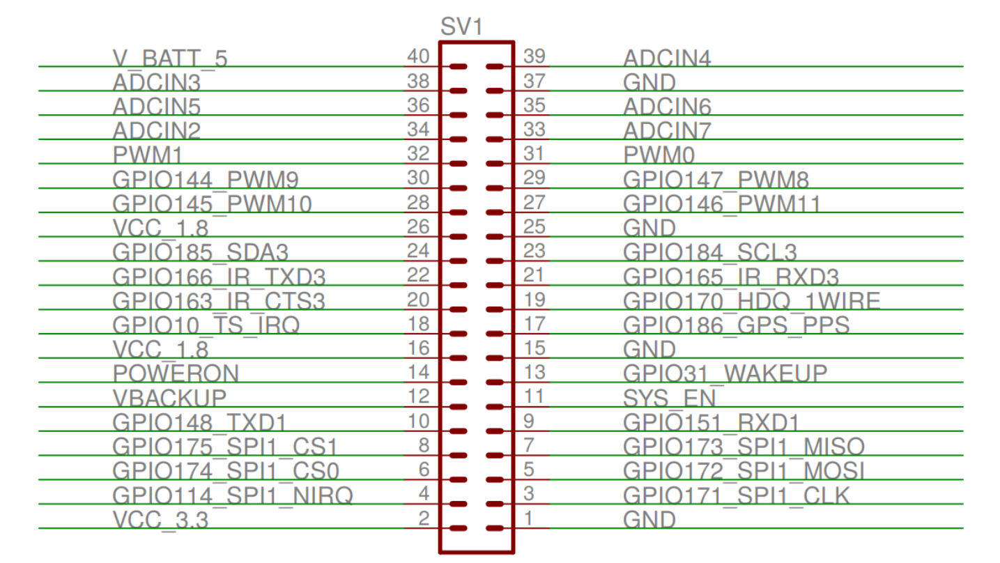
Tobi expansion board pin diagram.
GPIO control via terminal
The simplest, but least efficient way to control the GPIO is described on the manufacturer’s own website, available at Control Overo GPIO. They indicate to control the GPIO by the Linux system terminal itself through a sysfs system. The sysfs system is a system of files offered by the Linux kernel for control and communication with devices and drivers through the Linux terminal.
If, for example, we want to control GPIO10 output using this method to flash an LED, we need to export GPIO10 to the user space by typing 10 in the file /sys/class/gpio/export, which will generate a directory with other files for GPIO10 manipulation. Next, we must define its direction as outgoing by writing out in /sys/class/gpio/gpio10/direction and define its value as high or low by writing 1 or 0 in /sys/class/gpio/gpio10/value.
Tip
The interrupt configuration function is also accessible from the terminal.
This process can be done by the user’s terminal with the command echo, or by a program that opens this file and writes to it for us. For example, to control GPIO146 via the terminal, we can execute the following commands (example used on the Gumstix website):
Note
Remembering that the command echo test > folder/file will overwrite the entire file with the word ‘test’ and the command cat folder/file will display the contents of the file.
root@overo# echo 146 > /sys/class/gpio/export
root@overo:/sys/class/gpio# cat gpio146/direction
in
root@overo# echo out > /sys/class/gpio/gpio146/direction
root@overo:/sys/class/gpio# cat gpio146/direction
out
root@overo# cat /sys/class/gpio/gpio146/value
0
root@overo# echo 1 > /sys/class/gpio/gpio146/value
root@overo# cat /sys/class/gpio/gpio146/value
1
This command will control pin 27 on the Tobi board.
Tip
If you don’t have a meter, a 1.8V LED can be used. Use pin 1 as the ground.
However, as already mentioned, this method is very slow and cannot be used for communication between devices. Thought, for activities over 100 milliseconds, this method can be used smoothly.
Another approach, using the same method, is to use code similar to the code shown below, which writes directly to GPIO files. This approach has been tested and has considerably improved, through a simple code, the GPIO response time.
#include <stdio.h>
#include <string.h>
#include <stdlib.h>
#include <unistd.h>
#include <fcntl.h>
#include <termios.h>

int main()
{
    int arq = open("/sys/class/gpio/export", O_WRONLY);
    write(arq, "10", 2);
    close(arq);

    arq = open("/sys/class/gpio/gpio10/direction", O_WRONLY);
    write(arq, "out", 3);
    close(arq);

    arq = open("/sys/class/gpio/gpio10/value", O_RDWR);

    for (int i = 0; i < 10000; i++)
    {
        write(arq, "1", 1);
        //usleep (500000);
        write(arq, "0", 1);
        //usleep (500000) ;
    }
    close(arq);

    return 0;
}
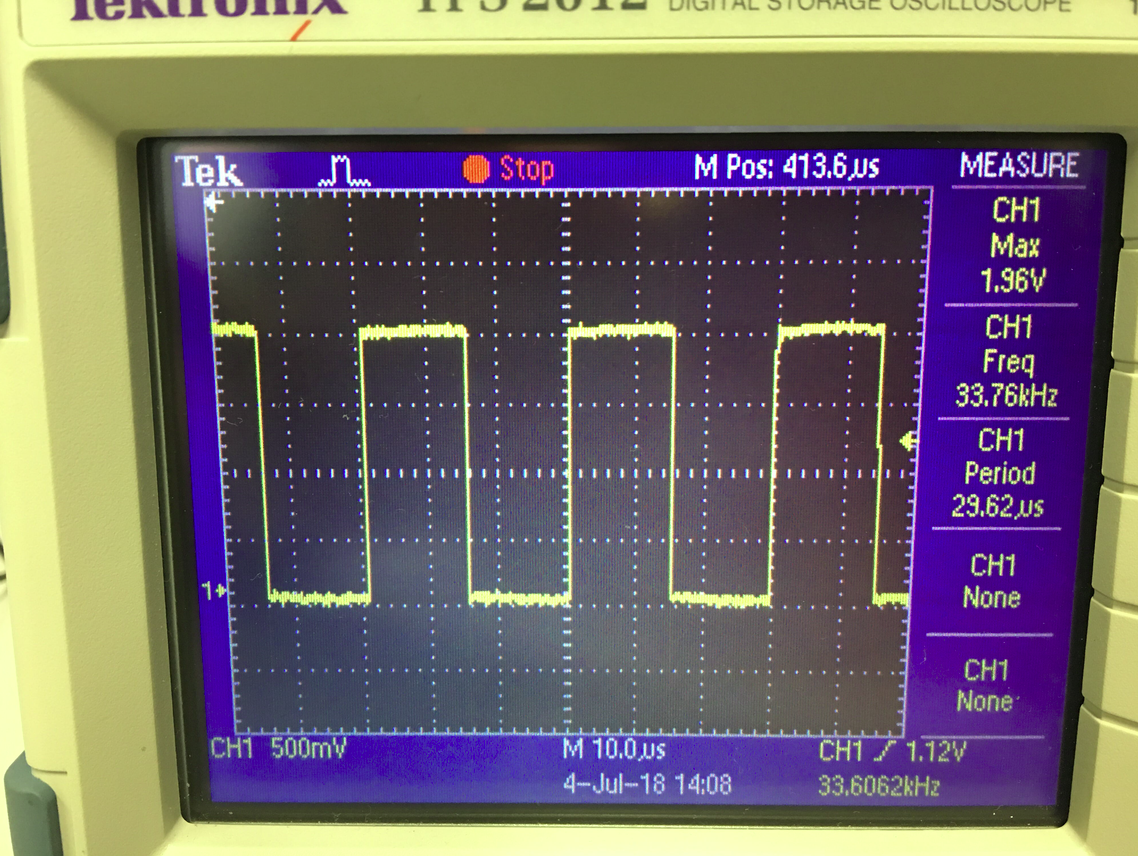
To test the code, pin 18 (GPIO pin 10) was connected to an oscilloscope in order to measure the period of the waveform. The result of this measurement can be seen in the figure below, in which we can see the amplitude of the wave form of 1.96 V, frequency of 33.76 kHz and period of 29.62 microseconds. For most applications we can use this method.
GPIO control via registers
Another way to control the GPIO is to write directly to the system registers. Although the procedure is a little more complex, this is actually the most common and recommended way to perform this procedure, offering much faster results.
To use this method, we first need to define which registers to write to and what to write to. This information can only be found at Technical Reference Manual (TRM) of the DM3730 processor, available on the Texas Instruments website.
As explained in section 25 of the DM3730 processor TRM, starting on page 3477, the control interface combines six GPIO banks. Each GPIO module provides 32 pins, totaling 192 pins that can be used as input and/or output. In our case, only some of these 192 pins are physically accessible, as can be seen in the figure shown below. Each GPIO bank has 26 registers distributed from a base address, each register having a length of 32 bits or 4 bytes.

Diagram of the GPIO interface.
Note
The figure was taken from the Technical Reference Manual of the DM3730 processor and shows a little more detail how these pins are distributed among the GPIO modules. A detailed explanation of each of these registers can be found in the DM3730 processor manual.
In this work, only two of the registers will be commented in order to illustrate the functioning of these registers.
The register GPIO_OE is the register that defines the direction of the pin being configured. The abbreviation “OE” comes from “Output Enable”. This register has an address offset equal to “0x034”, that is, its address will be the base address of the GPIO module plus 34 in hexadecimal. This register has 32 bits of type “Read/White”, or so, if the pin corresponding to the GPIO port is storing the value 0, this GPIO port will be configured to operate as an output, if this pin is the value 1 the port will be configured as an input.
The register GPIO_SETDATAOUT is the register that has the function of setting the bit corresponding to the register GPIO_DATAOUT to 1. That is, if everything is set correctly, the voltage value equivalent to bit 1 will appear on the physical pin. This register has an offset address equal to “0x094”. Like the register mentioned above, this register consists of 32 bits of type “RW”. Reading any of the bits in this register returns the value of the corresponding bit in GPIO_DATAOUT.
In addition to the registers shown in section 25 of the Technical Reference Manual, it’s also necessary to configure a register for the System Control Module (SCM). SCM is a module that allows control through software of various functions of the device. For our application, the SCM is the primary control point for the GPIO function and it is where we will perform the multiplexing, which determines whether the pin will operate in the GPIO function or in its specific function, and we will define whether the GPIO will be of the type pullup or pulldown, for example.
SCM registrars are divided into five classes. However, for our application we will use only one, the block of configuration and multiplexing registers. This block is a set of 32-bit registers, which configures 2 pins and defines, in addition to the two parameters mentioned above, the wakeup function. Registrars belonging to this block are called Configuration Register Functionality.
Note
More information about SCM can be found in section 13 of the Technical Reference Manual.
To find the address of each register of this type we can look in table 13-4 of the TRM. This table will be given the exact physical address of each register (base + offset). In this case, the base address is the address of the “PADCONFS” registers of the SCM interface, found in section 13.6.1 of the TRM and the offset address of each register in this block can be found in table 13-73 of the same document.
After the identification of the registrars, we can start the elaboration of a code to modify them. So we face yet another challenge, operating systems work with two concepts of memory, physical memory and virtual memory. Physical memory is the memory of the hardware, the one that we know the address and because we checked in the TRM. However, if we create a pointer that points to the memory “0x4800000”, for example, it will not point to the physical memory that has this address because the operating system maps a different physical memory space for each program with the main objectives of increasing the security and avoid data conflicts between programs.
However, to have access to the physical memory of the system, we need to ask the operating system to map this memory space to the application. One way to do this is through the ´´mmap ()´´ function.
Note
Details on how this function works and its parameters can be found at mmap(2) — Linux manual page.
Let’s assume that we want to map the physical memory space from 0x45000000 to 0x45001000 and for that we decided to use the mmap () function. Therefore, we call the function as follows, for example, mmap(NULL,0x1000,PROT_WRITE || PROT_READ,MAP_SHARED,fd,0x45000000), by executing this the function will return a pointer that points to a virtual memory address addressed to the physical memory address 0x45000000. Where, to access the physical memory of the device, “fd” is the file descriptor directed to “/dev/mem”.
With this information, we have everything that is necessary to implement tests on this operating mode. Below is a code that applies the method described in this section to toggle the voltage level of pin 186. This code was implemented to perform the same test as the section “GPIO control via terminal”.
Note
The code below was obtained from the Gumstix Discussion Forum and minor changes were made to avoid excessive information and facilitate its understanding.
// Local includes definition
#include <stdio.h>    // for lprint instruction
#include <stdlib.h>
#include <fcntl.h>    // ok for mmap
#include <sys/mman.h> // ok for mmap
#include <unistd.h>

// Defines local parameters (from TRM)
#define SCM_INTERFACE_BASE 0x48002000
#define SCM_PADCONFS_BASE 0x48002030
#define CONTROL_PADCONF_SYS_NIRQ (*(volatile unsigned long *)0x480021E0)
#define CONTROL_PADCONF_SYS_NIRQ_OFFSET 0x1B0

#define GPIO6_BASE 0x49058000
#define GPIO6_SYSCONFIG_OFFSET 0x10
#define GPIO6_CLEARDATAOUT_OFFSET 0x90
#define GPIO6_SETDATAOUT_OFFSET 0x94
#define GPIO6_OE_OFFSET 0x34
#define GPIO6_CTRL_OFFSET 0x30

#define MAP_SIZE (volatile unsigned long)4 * 1024
#define MAP_MASK (volatile unsigned long)(MAP_SIZE - 1)

// Defines "volatile unsigned long" how "u32"
#define u32 volatile unsigned long

// Defines commom variables
u32 *A;
u32 *B;

int main() // Local functions definition
{
    // Defines local variables
    unsigned long i;
    int fd;
    int j;

    fd = open("/dev/mem", O_RDWR | O_SYNC); // "O_RDWR" opens the file for reading and writing & "O_SYNC" guarantees that the call will not return before all data has been transferred to the disk

    A = (u32 *)mmap(NULL, MAP_SIZE, PROT_READ | PROT_WRITE, MAP_SHARED, fd, SCM_INTERFACE_BASE & ~MAP_MASK); // creates a new mapping in the virtual address space

    *(u32 *)((u32)A + 0x30 + CONTROL_PADCONF_SYS_NIRQ_OFFSET) |= (0x00040000); //set mode 4 on the pad 186 configuration register; enables digital pin use

    close(fd);
    /********/

    fd = open("/dev/mem", O_RDWR | O_SYNC);

    B = (volatile unsigned long *)mmap(NULL, MAP_SIZE, PROT_READ | PROT_WRITE, MAP_SHARED, fd, GPIO6_BASE & ~MAP_MASK); // COM1 0x4806A000

    //gpio_186 handling
    *(u32 *)((u32)B + GPIO6_SYSCONFIG_OFFSET) |= 0x00000004; // bit2=1 enable/wake up, free running clock

    //*(u32 *)((u32)B + GPIO6_CTRL_OFFSET) &= 0xfffffffe; // bit0=0 module enabled, clock not gated , clock=interface clock divided by 8

    *(u32 *)((u32)B+GPIO6_CTRL_OFFSET)&= 0xfffffff8;  // bit0=0,bit1=0,bit2=0 module enabled, clock not gated , clock=interface clock not divided

    *(u32 *)((u32)B + GPIO6_OE_OFFSET) &= 0xfbffffff; // bit26=0, gpio_186 output

    // generate a pulse stream on gpio_186 pin output

    for (j = 0; j < 1000000; j++)
    {
        *(u32 *)((u32)B + (GPIO6_CLEARDATAOUT_OFFSET)) |= 0x04000000;
        //printf("Saida = 0\n");
        //usleep(1000000);


        *(u32 *)((u32)B + (GPIO6_SETDATAOUT_OFFSET)) |= 0x04000000;
        //printf("Saida = 1\n");
        //usleep(1000000);
    }
    close(fd);
    return (0);
}
The code above was tested in the same way as the code presented in the previous section. In the following figure, you can see the result of this test. Note that the time obtained was 720.3 nanoseconds, that is, approximately 42 times faster than the result of the other method. Moreover, we can observe that the waveform is no longer an exact rectangular signal, the presence of a capacitive effect slowing the process is evident, therefore, it is possible that this is the maximum speed at which the signal of a pin can be changed .
Very hardly any application involving GPIO will not be satisfied by any of the methods presented here.
Problems writing to registers
To conclude this last topic, it is necessary to highlight some recently encountered problems involving writing in registers.
The first problem encountered occurs whenever we try to change the value of registers “0x49050030”, “0x49056030” and “0x49058030”, responsible for controlling the clock of the entire block of “GPIO_2”,”GPIO_5” and “GPIO_6”, respectively.
Note
devmem2 is a command that executes a simple program to read or write in any memory space. More information can be found in devmem2 - Ubuntu Manual.
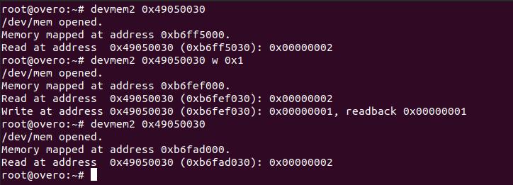
What happens is that moments after changing the value of the register, its returns the value it had before being changed. As the test in this section had a very high frequency, it was not interrupted by this effect, but the phenomenon occurs even when we change values of the registers by terminal commands, such as devmem2. This problem is exemplified in the figure below, where we execute the command devmem2 0x49058030 w 0x2 to modify the register 0x49058030 which is the register that controls the clock of the entire GPIO_6 block.
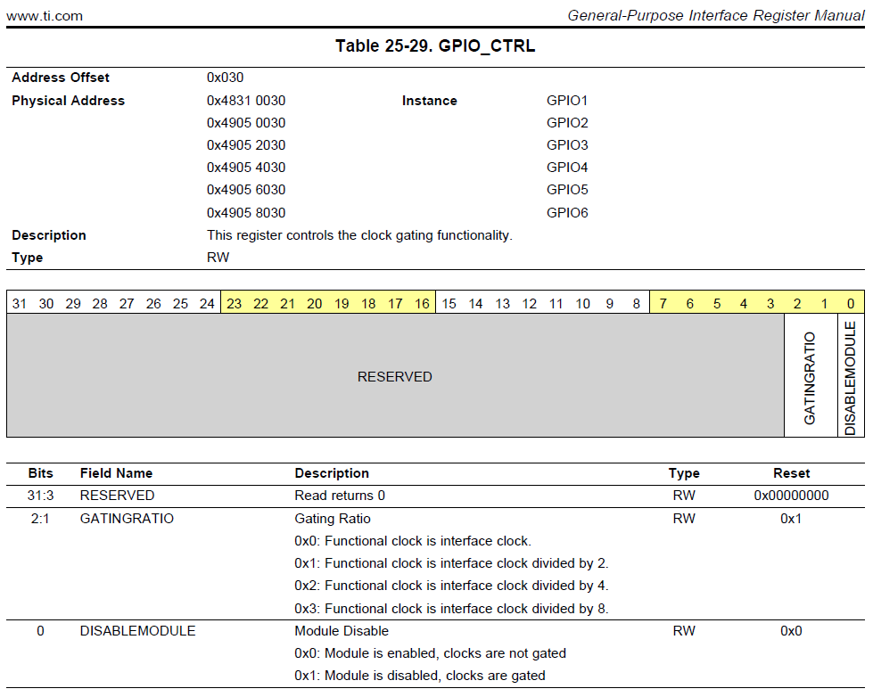
Such modification should reduce the clock speed by dividing it by 2, as indicated in the Technical Reference Manual (TRM) of the DM3730 processor, in table 25-29, page 3528, where it is explained that the GPIO_CTRL may have its clock divided by certain pre-registered values, as shown in the following figure.
However, immediately after executing the command, a reading procedure is performed that ensures that everything was written in the register as expected. Though, the same command, executed moments later in read mode, always returns to the previously stored value, the value existing in the register before the modification. It’s worth mentioning that this problem doesn’t occur for the GPIO control method via terminal, this method operates until it receives a stop order from the user.
The second problem found occurs when we try to change the value of the registers 0x49052030 and 0x49054030, responsible for controlling the clock of the entire block of GPIO_3 and GPIO_4, respectively. In these specific registers, when trying to execute the command devmem2 to change the clock of a given GPIO block or just perform a reading, the system returns the error “bus error” as shown in the figure below, where we execute the same command in register 0x49054030.

Thus, it was only possible to change the GPIO_1 block clock, as can be seen in the image below.

We do not know why these phenomena are occurring with blocks 2 to 6, but suspect that some processes of the operating system are preventing the clock of such blocks from being changed, probably by some internal circuit or operation depends on such pre-defined values or even some restriction on energy consumption.
References
- PITA, H. C. Desenvolvimento de sistema de comunicação multiplataforma para veículos aéreos de asa fixa. Faculdade de Tecnologia, Universidade de Brasília, 2018.
- TEXAS INSTRUMENTS. AM/DM37x Multimedia Device Technical Reference Manual. 12500 TI Blvd, Dallas, TX 75243, EUA, 2012. Version R. Disponível em: ti.com.
- Direct register access control of GPIO ARM interface on Overo Water +TOBI - Gumstix Discussion Forum